- 您现在的位置:买卖IC网 > Sheet目录3855 > PIC16LC711-04/SS (Microchip Technology)IC MCU OTP 1KX14 A/D 20SSOP
112
7593L–AVR–09/12
AT90USB64/128
strobe. Therefore it is the value present in the COM0B1:0 bits that determines the effect of the
forced compare.
A FOC0B strobe will not generate any interrupt, nor will it clear the timer in CTC mode using
OCR0B as TOP.
The FOC0B bit is always read as zero.
Bits 5:4 – Res: Reserved bits
These bits are reserved bits and will always read as zero.
Bit 3 – WGM02: Waveform Generation Mode
See the description in the “TCCR0A – Timer/Counter Control Register A” on page 108.
Bits 2:0 – CS02:0: Clock Select
The three Clock Select bits select the clock source to be used by the Timer/Counter.
If external pin modes are used for the Timer/Counter0, transitions on the T0 pin will clock the
counter even if the pin is configured as an output. This feature allows software control of the
counting.
14.8.3
TCNT0 – Timer/Counter Register
The Timer/Counter Register gives direct access, both for read and write operations, to the
Timer/Counter unit 8-bit counter. Writing to the TCNT0 Register blocks (removes) the Compare
Match on the following timer clock. Modifying the counter (TCNT0) while the counter is running,
introduces a risk of missing a Compare Match between TCNT0 and the OCR0x Registers.
14.8.4
OCR0A – Output Compare Register A
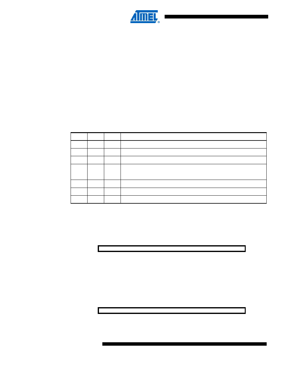
Table 14-8.
Clock Select bit description.
CS02
CS01
CS00
Description
0
No clock source (Timer/Counter stopped)
001
clkI/O/(No prescaling)
010
clkI/O/8 (From prescaler)
011
clkI/O/64 (From prescaler)
100
clkI/O/256 (From prescaler)
101
clkI/O/1024 (From prescaler)
1
0
External clock source on T0 pin. Clock on falling edge.
1
External clock source on T0 pin. Clock on rising edge.
Bit
7
65
43
21
0
TCNT0[7:0]
TCNT0
Read/write
R/W
Initial value
00
Bit
7
65
43
21
0
OCR0A[7:0]
OCR0A
Read/write
R/W
Initial value
00
发布紧急采购,3分钟左右您将得到回复。
相关PDF资料
PIC18F65K22-I/MRRSL
MCU PIC 32K FLASH MEM XLP 64QFN
PIC16LF87-I/SS
IC MCU FLASH 4KX14 EEPROM 20SSOP
PIC16C62B-20/SS
IC MCU OTP 2KX14 PWM 28SSOP
PIC16LC711-04I/SO
IC MCU OTP 1KX14 A/D 18SOIC
PIC18F66J90-I/PT
IC PIC MCU FLASH 64KB 64-TQFP
ATMEGA32L-8AC
IC AVR MCU 32K LV 8MHZ COM44TQFP
DSPIC30F2012-30I/SP
IC DSPIC MCU/DSP 12K 28DIP
PIC18LF2321-I/ML
IC PIC MCU FLASH 4KX16 28QFN
相关代理商/技术参数
PIC16LC711-04E/P
功能描述:8位微控制器 -MCU 1.75KB 68 RAM 13 I/O RoHS:否 制造商:Silicon Labs 核心:8051 处理器系列:C8051F39x 数据总线宽度:8 bit 最大时钟频率:50 MHz 程序存储器大小:16 KB 数据 RAM 大小:1 KB 片上 ADC:Yes 工作电源电压:1.8 V to 3.6 V 工作温度范围:- 40 C to + 105 C 封装 / 箱体:QFN-20 安装风格:SMD/SMT
PIC16LC711-04E/SO
功能描述:8位微控制器 -MCU 1.75KB 68 RAM 13 I/O RoHS:否 制造商:Silicon Labs 核心:8051 处理器系列:C8051F39x 数据总线宽度:8 bit 最大时钟频率:50 MHz 程序存储器大小:16 KB 数据 RAM 大小:1 KB 片上 ADC:Yes 工作电源电压:1.8 V to 3.6 V 工作温度范围:- 40 C to + 105 C 封装 / 箱体:QFN-20 安装风格:SMD/SMT
PIC16LC711-04E/SS
功能描述:8位微控制器 -MCU 1.75KB 68 RAM 13 I/O RoHS:否 制造商:Silicon Labs 核心:8051 处理器系列:C8051F39x 数据总线宽度:8 bit 最大时钟频率:50 MHz 程序存储器大小:16 KB 数据 RAM 大小:1 KB 片上 ADC:Yes 工作电源电压:1.8 V to 3.6 V 工作温度范围:- 40 C to + 105 C 封装 / 箱体:QFN-20 安装风格:SMD/SMT
PIC16LC711-04I/P
功能描述:8位微控制器 -MCU 1.75KB 68 RAM 13 I/O RoHS:否 制造商:Silicon Labs 核心:8051 处理器系列:C8051F39x 数据总线宽度:8 bit 最大时钟频率:50 MHz 程序存储器大小:16 KB 数据 RAM 大小:1 KB 片上 ADC:Yes 工作电源电压:1.8 V to 3.6 V 工作温度范围:- 40 C to + 105 C 封装 / 箱体:QFN-20 安装风格:SMD/SMT
PIC16LC711-04I/P
制造商:Microchip Technology Inc 功能描述:IC 8BIT CMOS MCU 16LC711 DIP18
PIC16LC711-04I/SO
功能描述:8位微控制器 -MCU 1.75KB 68 RAM 13 I/O RoHS:否 制造商:Silicon Labs 核心:8051 处理器系列:C8051F39x 数据总线宽度:8 bit 最大时钟频率:50 MHz 程序存储器大小:16 KB 数据 RAM 大小:1 KB 片上 ADC:Yes 工作电源电压:1.8 V to 3.6 V 工作温度范围:- 40 C to + 105 C 封装 / 箱体:QFN-20 安装风格:SMD/SMT
PIC16LC711-04I/SO
制造商:Microchip Technology Inc 功能描述:8BIT CMOS MCU SMD 16LC711 SOIC18
PIC16LC711-04I/SS
功能描述:8位微控制器 -MCU 1.75KB 68 RAM 13 I/O RoHS:否 制造商:Silicon Labs 核心:8051 处理器系列:C8051F39x 数据总线宽度:8 bit 最大时钟频率:50 MHz 程序存储器大小:16 KB 数据 RAM 大小:1 KB 片上 ADC:Yes 工作电源电压:1.8 V to 3.6 V 工作温度范围:- 40 C to + 105 C 封装 / 箱体:QFN-20 安装风格:SMD/SMT